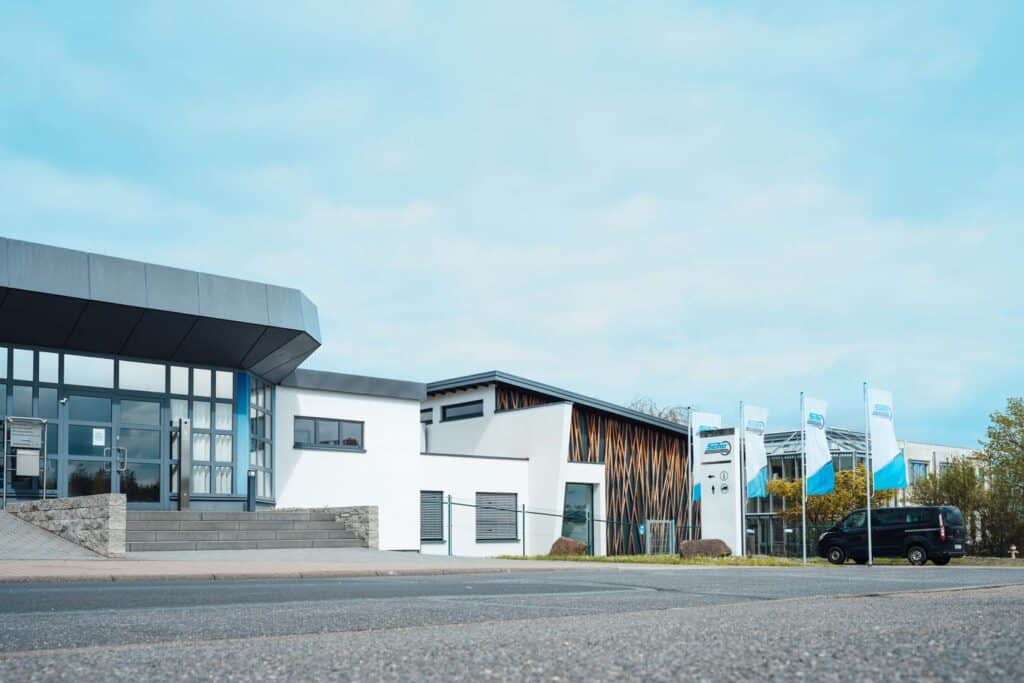
Welcome at SEHO!
We are the specialist for soldering processes and automatic production lines. Our customers benefit from total solutions that convince through flexibility, performance and efficiency.
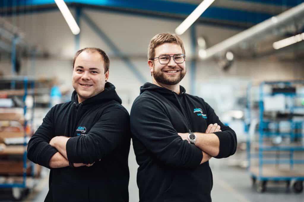
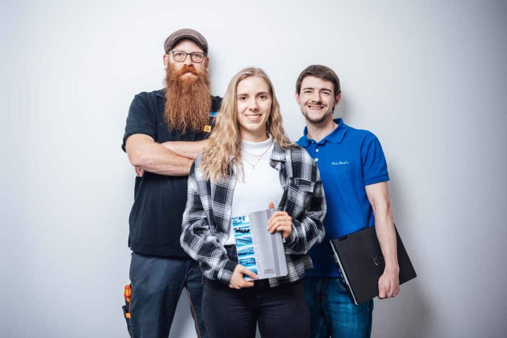
SEHO, that's us!
A great team with a variety of personalities. We work together for our success of tomorrow.
SEHO also stands for Sustainability.
German mechanical engineering plays a central role in implementing the EU Green Deal. But what does SEHO contribute to the preservation of our environment? You can find out all about it in our report on environmental management.
0
+
wonderful employees
only
7
working days per week
0
+
machines in the last two years
We are a multi-award-winning technology leader and have received the Global Technology Award several times in recent years.
Upcoming Events
No event found!